
Preview
基本信息产品详情证书
基本信息
| 型号/编号 | 12 英寸 |
| 成长法 | CZ |
| 晶体取向 | 100 |
| 杂质 | 硼 |
| 电阻率 | 1-100欧姆 |
| 前侧 | 精致的 |
| Edge | 抛光 |
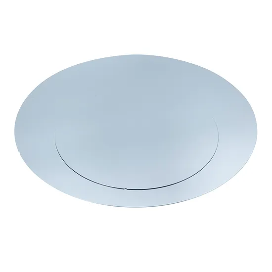
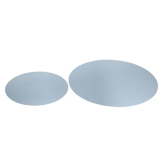
| 直径 | 300毫米正负0.2毫米 |
| 厚度 | 775±25微米 |
| 运输包 | 半标准 |
| 规格 | TBD |
| 商标 | FSM |
| 起源 | 中国 |
| 商品编码 | 3818001920 |
| 生产能力 | 每月5000件 |
产品详情
Product Description
Preview
Why Choose FSM?
Expertise : With a team of seasoned professionals and cutting-edge manufacturing facilities, we consistently deliver wafers of the highest quality.Wide Range of Products : Whether you require Czochralski (CZ) and Float Zone (FZ) silicon wafers or SOI and glass wafers, our extensive product lineup is designed to cater to your every need.Customization : Our specialty lies in crafting custom wafers tailored precisely to your specifications, ensuring the seamless success of your project.Fast Turnaround : Thanks to our streamlined processes and well-stocked inventory, we guarantee swift delivery to keep your projects on track.Global Reach : Delivering worldwide from our strategic hubs in China and Japan, we proudly serve a diverse clientele in over 50 countries.
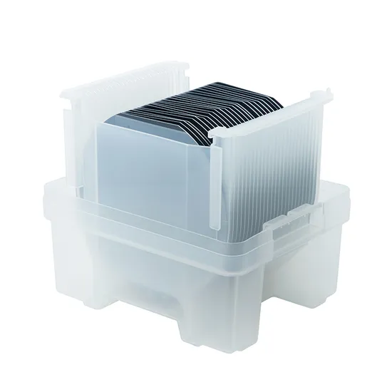
Dummy wafers, also known as test wafers, are primarily utilized for experimental and testing purposes, differing from standard wafers used in products.Reclaimed wafers are predominantly employed as dummy wafers (test wafers).Dummy wafers are frequently utilized in production devices to enhance safety at the outset of the production process and are critical for delivery checks and process evaluation.Given their role in experimentation and testing, the size and thickness of dummy wafers are crucial factors in most scenarios.
Wafers that undergo film deposition are referred to as film wafers.Examples of films used include isolation films for inter-layer separation, metal films for conductivity, and process materials like resist and protective films.
Product Parameters
Use Reference Value
150MM/200MM Test Wafer - Perfect for innovative testing applications.
300MM Test Wafer - Ideal for comprehensive testing needs in advanced research.
200MM/300MM Oxide Wafer - Suitable for cutting-edge oxide applications.
* For any additional film types, film thickness, or composition inquiries, please feel free to contact us. Our expert team is here to assist you with tailored solutions.
Expertise : With a team of seasoned professionals and cutting-edge manufacturing facilities, we consistently deliver wafers of the highest quality.Wide Range of Products : Whether you require Czochralski (CZ) and Float Zone (FZ) silicon wafers or SOI and glass wafers, our extensive product lineup is designed to cater to your every need.Customization : Our specialty lies in crafting custom wafers tailored precisely to your specifications, ensuring the seamless success of your project.Fast Turnaround : Thanks to our streamlined processes and well-stocked inventory, we guarantee swift delivery to keep your projects on track.Global Reach : Delivering worldwide from our strategic hubs in China and Japan, we proudly serve a diverse clientele in over 50 countries.
Dummy wafers, also known as test wafers, are primarily utilized for experimental and testing purposes, differing from standard wafers used in products.Reclaimed wafers are predominantly employed as dummy wafers (test wafers).Dummy wafers are frequently utilized in production devices to enhance safety at the outset of the production process and are critical for delivery checks and process evaluation.Given their role in experimentation and testing, the size and thickness of dummy wafers are crucial factors in most scenarios.
Wafers that undergo film deposition are referred to as film wafers.Examples of films used include isolation films for inter-layer separation, metal films for conductivity, and process materials like resist and protective films.
Product Parameters
Use Reference Value
150MM/200MM Test Wafer - Perfect for innovative testing applications.
300MM Test Wafer - Ideal for comprehensive testing needs in advanced research.
200MM/300MM Oxide Wafer - Suitable for cutting-edge oxide applications.
* For any additional film types, film thickness, or composition inquiries, please feel free to contact us. Our expert team is here to assist you with tailored solutions.
Preview
Certifications
Preview
Packaging & Shipping
Preview
Company Profile
Preview

Preview
Since its inception in August 2008, Fine Silicon Manufacturing (Shanghai) Ltd. has carved a niche in the wafer reclaim industry. Strategically located in the bustling heart of Shanghai's Pudong New Area, our state-of-the-art facility specializes in the meticulous lapping and polishing of 6-12 inch silicon wafers. Boasting an impressive production capacity of 50,000 pieces per month, we stand at the forefront of innovation and efficiency. As a trusted agent, we also offer expert services in particle-controlled test wafer reclaim, advanced wafer film coating, and precision wafer thinning techniques. For those seeking unparalleled quality and service, we invite you to CONTACT US for comprehensive information and tailored solutions.
Our Advantages
Our Advantages
Preview
FAQ
Preview
Q: What shipping methods are available?A: We proudly offer a variety of shipping options, including DHL, FedEx, TNT, UPS, EMS, SF, and more.Q: What are the accepted payment methods?A: We accept T/T and PayPal as payment methods, along with other options as needed.Q: How long is the delivery time?A: For products in stock, expect a swift delivery time of just 5 business days.For customized orders, delivery is typically within 7 to 25 business days, depending on the quantity required.Q: Is product customization available to suit my needs?A: Absolutely! We can tailor the material, specifications, and optical coating of your optical components to meet your specific requirements.Each customer has unique specifications, and Fine Silicon Manufacturing (Shanghai) Ltd. is dedicated to providing wafers that match your precise needs.If your desired specification is not listed, please CONTACT FSM to connect with our experienced and knowledgeable sales team for personalized assistance.
Preview
证书
标题:SGS认证证书

Preview


 上海
上海  已认证
已认证