


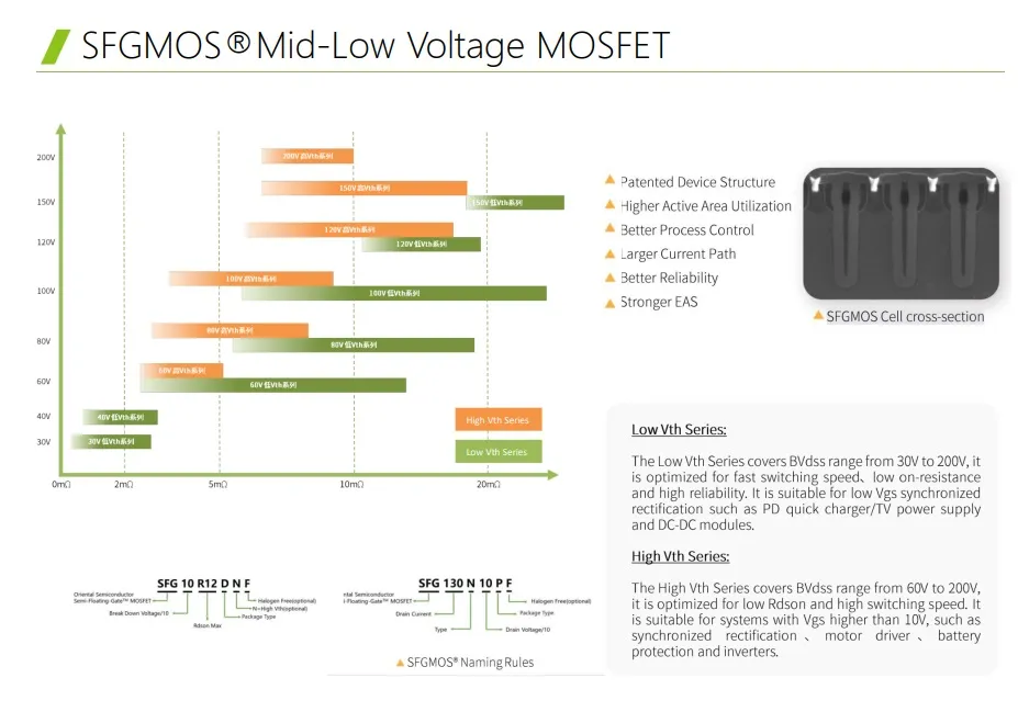
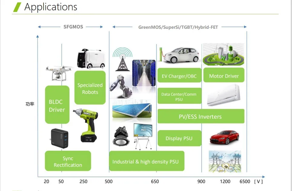
Preview
基本信息产品详情证书
基本信息
| 型号编号 | OSG80R900DF TO252-1 |
| 材料 | 元素半导体 |
| 模型 | 装货单 |
| 包裹 | SMD |
| 信号处理 | 模拟数字复合与功能 |
| 类型 | N型半导体 |
| 应用程序1 | LED照明 |
| 应用程序2 | 电动汽车充电器 |
| P/N | Osg80r900df |
| 包装 | To252 |
| 品牌 | 东方萨米 |
| 运输包 | 纸箱 |
| 规格说明 | 35x30x37厘米 |
| 商标 | 奥瑞安赛米 |
| 起源 | 中国 |
| 商品编码 | 8541290000 |
| 生产能力 | 每月收入超过一千元 |
| 包装尺寸 | 59.00厘米×39.00厘米×16.00厘米 |
| 包装总重量 | 19000千克 |
| 包装尺寸 | 59.00cm * 39.00cm * 16.00cm |
| 包装总重量 | 19.000千克 |
产品详情
Product Description
Preview
General
Description
The GreenMOS®
high voltage
MOSFET
utilizes charge
balance technology to
achieve
outstanding
low
on-resistance
and
lower
gate
charge.It
is
engineered
to
minimize
conduction
loss,
provide
superior switching
performance and
robust avalanche capability.
The
GreenMOS®
Generic
series
is
optimized
for
extreme
switching
performance
to
minimize
switching
loss.It
is
tailored
for
high
power
density
applications
to
meet
the
highest
efficiency standards.
Features
.Low
RDS(ON)
&
FOM
.Extremely
low switching
loss
.Excellent stability and
uniformity
Applications
.PC
power
.LED
lighting
.Telecom
power
.Server
power
.EV
Charger
.Solar/UPS
Key Performance
Parameters
General
DescriptionThe GreenMOS®
high voltage
MOSFET
utilizes charge
balance technology to
achieve
outstanding
low
on-resistance
and
lower
gate
charge.It
is
engineered
to
minimize
conduction
loss,
provide
superior switching
performance and
robust avalanche capability.The
GreenMOS®
Generic
series
is
optimized
for
extreme
switching
performance
to
minimize
switching
loss.It
is
tailored
for
high
power
density
applications
to
meet
the
highest
efficiency standards.Features.Low
RDS(ON)
&
FOM.Extremely
low switching
loss.Excellent stability and
uniformityApplications.PC
power.LED
lighting.Telecom
power.Server
power.EV
Charger.Solar/UPSKey Performance
Parameters
Marking
Information
Parameter
Symbol
Value
Unit
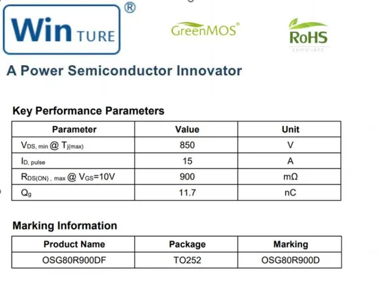
Drain-source voltage
VDS
800
V
Gate-source voltage
VGS
±30
Continuous
drain
current1)
, TC=25
°C
ID
5
A
, TC=100
3.2
Pulsed
current2)
ID,
pulse
15
diode
forward
IS
Diode
pulsed
IS,
Power
dissipation3)
, TC=25 °C
PD
63
W
Single pulsed avalanche
energy5)
EAS
160
mJ
MOSFET
dv/dt
ruggedness, VDS=0…640 V
50
V/ns
Reverse
dv/dt, VDS=0…640 V,
ISD≤ID
Operation and storage temperature
Tstg, Tj
-55 to
150
Thermal resistance,
junction-case
RθJC
2
°C/W
junction-ambient4)
RθJA
62
Dynamic Characteristics
Gate Charge Characteristics
Body Diode Characteristics
Note1)
Calculated continuous current
based
on
maximum
allowable junction temperature.2)
Repetitive
rating;
pulse width
limited
by
max. junction temperature.3)
Pd
is
based on
max. junction temperature,
using junction-case thermal resistance.4)
The
value
of
RθJA
is
measured
with
the
device
mounted
on
1
in
2
FR-4
board
with
2oz.Copper,
in
a
still
air
environment
with
Ta=25
°C.5)
VDD=100 V, VGS=10 V,
L=60
mH, starting
Tj=25
°C.Supply Chain
Description
The GreenMOS®
high voltage
MOSFET
utilizes charge
balance technology to
achieve
outstanding
low
on-resistance
and
lower
gate
charge.It
is
engineered
to
minimize
conduction
loss,
provide
superior switching
performance and
robust avalanche capability.
The
GreenMOS®
Generic
series
is
optimized
for
extreme
switching
performance
to
minimize
switching
loss.It
is
tailored
for
high
power
density
applications
to
meet
the
highest
efficiency standards.
Features
.Low
RDS(ON)
&
FOM
.Extremely
low switching
loss
.Excellent stability and
uniformity
Applications
.PC
power
.LED
lighting
.Telecom
power
.Server
power
.EV
Charger
.Solar/UPS
Key Performance
Parameters
General
DescriptionThe GreenMOS®
high voltage
MOSFET
utilizes charge
balance technology to
achieve
outstanding
low
on-resistance
and
lower
gate
charge.It
is
engineered
to
minimize
conduction
loss,
provide
superior switching
performance and
robust avalanche capability.The
GreenMOS®
Generic
series
is
optimized
for
extreme
switching
performance
to
minimize
switching
loss.It
is
tailored
for
high
power
density
applications
to
meet
the
highest
efficiency standards.Features.Low
RDS(ON)
&
FOM.Extremely
low switching
loss.Excellent stability and
uniformityApplications.PC
power.LED
lighting.Telecom
power.Server
power.EV
Charger.Solar/UPSKey Performance
Parameters
Marking
Information
Parameter
Symbol
Value
Unit
Drain-source voltage
VDS
800
V
Gate-source voltage
VGS
±30
Continuous
drain
current1)
, TC=25
°C
ID
5
A
, TC=100
3.2
Pulsed
current2)
ID,
pulse
15
diode
forward
IS
Diode
pulsed
IS,
Power
dissipation3)
, TC=25 °C
PD
63
W
Single pulsed avalanche
energy5)
EAS
160
mJ
MOSFET
dv/dt
ruggedness, VDS=0…640 V
50
V/ns
Reverse
dv/dt, VDS=0…640 V,
ISD≤ID
Operation and storage temperature
Tstg, Tj
-55 to
150
Thermal resistance,
junction-case
RθJC
2
°C/W
junction-ambient4)
RθJA
62
Dynamic Characteristics
Gate Charge Characteristics
Body Diode Characteristics
Note1)
Calculated continuous current
based
on
maximum
allowable junction temperature.2)
Repetitive
rating;
pulse width
limited
by
max. junction temperature.3)
Pd
is
based on
max. junction temperature,
using junction-case thermal resistance.4)
The
value
of
RθJA
is
measured
with
the
device
mounted
on
1
in
2
FR-4
board
with
2oz.Copper,
in
a
still
air
environment
with
Ta=25
°C.5)
VDD=100 V, VGS=10 V,
L=60
mH, starting
Tj=25
°C.Supply Chain
Preview

Preview
Green Product Declaration
Preview

Preview
Preview
Preview
Preview

Preview
Preview
证书
标题:专利奖励

Preview
N通道800瓦900伏功率MOSFET器件(双252封装)Osg80r900df
¥0.72 ~ ¥3.62
消费电子产业链 · 半导体 · N型半导体
品牌东方萨米
产地中国


 上海
上海  已认证
已认证供应商其他热门产品


价格待议
价格待议
价格待议