


Preview
基本信息产品详情证书
基本信息
| 型号编号 | OSG80R300JF |
| 材料 | 化合物半导体 |
| Model | Osg80r300jf |
| 包装 | QFP和PFP |
| 信号处理 | 模拟数字复合与功能 |
| 类型 | N型半导体 |
| 应用程序1 | 书信电报 |
| 应用程序2 | LED照明 |
| 应用程序3 | 电信电源 |
| 应用程序4 | 太阳能/不间断电源 |
| 应用程序5 | 伺服电源 |
| 应用程序6 | 电脑电源 |
| 品牌 | 东方半壁 |
| 交通政策包 | 空气 |
| 商标 | Orientalsemi |
| 起源 | 中国 |
| 商品编码 | 八十五亿四千一百二十九万 |
| 生产能力 | 每月超过1kk |
| 包装尺寸 | 59.00cm * 3.00cm * 15.00cm |
| 包装总重量 | 18000千克 |
| 包装尺寸 | 59.00厘米乘以3.00厘米乘以15.00厘米 |
| 包装总重量 | 18千克 |
产品详情
Product Description
Preview
General Description
The
high voltage MOSFET utilizes charge balance technology to achieve outstanding low on-resistance and lower gate charge. It is engineered to minimize conduction loss, provide superior switching performance and robust avalanche capability. The
Generic series is optimized for extreme switching performance to minimize switching loss. It is tailored for high power density applications to meet the highest efficiency standards.
Features
Low
RDS(ON) &
FOM
Extremely
low
switching
loss
Excellent
stability
and
uniformity
Applications
LED
lighting
Telecom Power
Solar/UPS
Sever power
PC power
EV Charger
General Description
The
high voltage MOSFET utilizes charge balance technology to achieve outstanding low on-resistance and lower gate charge. It is engineered to minimize conduction loss, provide superior switching performance and robust avalanche capability. The
Generic series is optimized for extreme switching performance to minimize switching loss. It is tailored for high power density applications to meet the highest efficiency standards.Features
Low
RDS(ON) &
FOM
Extremely
low
switching
loss
Excellent
stability
and
uniformityApplications
LED
lighting
Telecom Power
Solar/UPS
Sever power
PC power
EV Charger
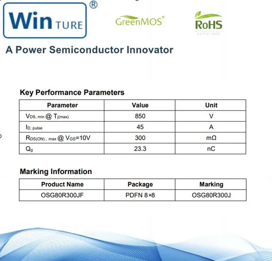
Key Performance
Parameters
Parameter
Value
Unit
VDS,
min
@ Tj(max)
850
V
ID,
pulse
45
A
RDS(ON)
,
max
@ VGS=10V
300
mΩ
Qg
23.3
nC
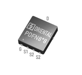
Marking
Information
Product
Name
Package
Marking
OSG80R300JF
PDFN
8×8
OSG80R300J
Package &
Pin
Information
Parameter
Symbol
Value
Unit
Drain-source voltage
VDS
800
V
Gate-source voltage
VGS
±30
Continuous
drain
current1)
, TC=25
°C
ID
15
A
, TC=100
9.5
Pulsed
current2)
ID,
pulse
45
diode
forward
IS
Diode
pulsed
IS,
Power
dissipation3)
, TC=25 °C
PD
151
W
Single pulsed avalanche
energy5)
EAS
360
mJ
MOSFET
dv/dt
ruggedness, VDS=0…480 V
50
V/ns
Reverse
dv/dt, VDS=0…480 V,
ISD≤ID
Operation and storage temperature
Tstg, Tj
-55 to
150
Thermal resistance,
junction-case
RθJC
0.83
°C/W
Thermal resistance, junction-ambient4)
RθJA
62
Dynamic Characteristics
Parameter
Symbol
Min.Typ.Max.Unit
Test condition
Input capacitance
Ciss
1552
pF
VGS=0 V,VDS=50 V,ƒ=100
kHz
Output capacitance
Coss
80.1
pF
Reverse transfer capacitance
Crss
2.1
pF
Turn-on delay time
td(on)
33.6
ns
VGS=10 V,VDS=400 V,RG=2
Ω,ID=7.5 A
Rise time
tr
20.3
ns
Turn-off delay time
td(off)
57.9
ns
Fall time
tf
4.5
ns
Gate Charge Characteristics
Parameter
Symbol
Min.Typ.Max.Unit
Test condition
Total gate
charge
Qg
22.7
nC
VGS=10 V,VDS=400 V,ID=7.5 A
Gate-source charge
Qgs
8.6
nC
Gate-drain charge
Qgd
2.3
nC
Gate plateau
voltage
Vplateau
5.5
V
Body Diode
Characteristics
Parameter
Symbol
Min.Typ.Max.Unit
Test condition
Diode forward voltage
VSD
1.3
V
IS=15 A,VGS=0 V
Reverse recovery time
trr
313.7
ns
VR
=400 V,IS=7.5 A,di/dt=100 A/μs
Reverse recovery charge
Qrr
4.2
μC
Peak
reverse
recovery current
Irrm
25.2
A
Note1)
Calculated continuous current
based
on
maximum
allowable junction temperature.2)
Repetitive
rating;
pulse width
limited
by
max. junction temperature.3)
Pd
is
based on
max. junction temperature,
using junction-case thermal resistance.4)
The
value
of
RθJA
is
measured
with
the
device
mounted
on
1
in
2
FR-4
board
with
2oz.Copper,
in
a
still
air
environment
with
Ta=25
°C.5)
VDD=100 V, VGS=10 V,
L=80
mH, starting
Tj=25
°Supply Chain
The
high voltage MOSFET utilizes charge balance technology to achieve outstanding low on-resistance and lower gate charge. It is engineered to minimize conduction loss, provide superior switching performance and robust avalanche capability. The
Generic series is optimized for extreme switching performance to minimize switching loss. It is tailored for high power density applications to meet the highest efficiency standards.
Features
Low
RDS(ON) &
FOM
Extremely
low
switching
loss
Excellent
stability
and
uniformity
Applications
LED
lighting
Telecom Power
Solar/UPS
Sever power
PC power
EV Charger
General Description
The
high voltage MOSFET utilizes charge balance technology to achieve outstanding low on-resistance and lower gate charge. It is engineered to minimize conduction loss, provide superior switching performance and robust avalanche capability. The
Generic series is optimized for extreme switching performance to minimize switching loss. It is tailored for high power density applications to meet the highest efficiency standards.Features
Low
RDS(ON) &
FOM
Extremely
low
switching
loss
Excellent
stability
and
uniformityApplications
LED
lighting
Telecom Power
Solar/UPS
Sever power
PC power
EV Charger
Key Performance
Parameters
Parameter
Value
Unit
VDS,
min
@ Tj(max)
850
V
ID,
pulse
45
A
RDS(ON)
,
max
@ VGS=10V
300
mΩ
Qg
23.3
nC
Marking
Information
Product
Name
Package
Marking
OSG80R300JF
PDFN
8×8
OSG80R300J
Package &
Pin
Information
Parameter
Symbol
Value
Unit
Drain-source voltage
VDS
800
V
Gate-source voltage
VGS
±30
Continuous
drain
current1)
, TC=25
°C
ID
15
A
, TC=100
9.5
Pulsed
current2)
ID,
pulse
45
diode
forward
IS
Diode
pulsed
IS,
Power
dissipation3)
, TC=25 °C
PD
151
W
Single pulsed avalanche
energy5)
EAS
360
mJ
MOSFET
dv/dt
ruggedness, VDS=0…480 V
50
V/ns
Reverse
dv/dt, VDS=0…480 V,
ISD≤ID
Operation and storage temperature
Tstg, Tj
-55 to
150
Thermal resistance,
junction-case
RθJC
0.83
°C/W
Thermal resistance, junction-ambient4)
RθJA
62
Dynamic Characteristics
Parameter
Symbol
Min.Typ.Max.Unit
Test condition
Input capacitance
Ciss
1552
pF
VGS=0 V,VDS=50 V,ƒ=100
kHz
Output capacitance
Coss
80.1
pF
Reverse transfer capacitance
Crss
2.1
pF
Turn-on delay time
td(on)
33.6
ns
VGS=10 V,VDS=400 V,RG=2
Ω,ID=7.5 A
Rise time
tr
20.3
ns
Turn-off delay time
td(off)
57.9
ns
Fall time
tf
4.5
ns
Gate Charge Characteristics
Parameter
Symbol
Min.Typ.Max.Unit
Test condition
Total gate
charge
Qg
22.7
nC
VGS=10 V,VDS=400 V,ID=7.5 A
Gate-source charge
Qgs
8.6
nC
Gate-drain charge
Qgd
2.3
nC
Gate plateau
voltage
Vplateau
5.5
V
Body Diode
Characteristics
Parameter
Symbol
Min.Typ.Max.Unit
Test condition
Diode forward voltage
VSD
1.3
V
IS=15 A,VGS=0 V
Reverse recovery time
trr
313.7
ns
VR
=400 V,IS=7.5 A,di/dt=100 A/μs
Reverse recovery charge
Qrr
4.2
μC
Peak
reverse
recovery current
Irrm
25.2
A
Note1)
Calculated continuous current
based
on
maximum
allowable junction temperature.2)
Repetitive
rating;
pulse width
limited
by
max. junction temperature.3)
Pd
is
based on
max. junction temperature,
using junction-case thermal resistance.4)
The
value
of
RθJA
is
measured
with
the
device
mounted
on
1
in
2
FR-4
board
with
2oz.Copper,
in
a
still
air
environment
with
Ta=25
°C.5)
VDD=100 V, VGS=10 V,
L=80
mH, starting
Tj=25
°Supply Chain
Preview

Preview
Green Product Declaration
Preview

Preview
Preview
Preview
Preview

Preview
Preview
Preview
证书
标题:专利奖励

Preview
太阳能/不间断电源高压单N沟道功率MOSFET
¥0.72 ~ ¥3.62
消费电子产业链 · 半导体 · N型半导体
品牌东方半壁
产地中国


 上海
上海  已认证
已认证供应商其他热门产品


价格待议
价格待议
价格待议